
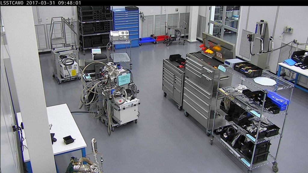
The race to produce more powerful processors is increasingly decided not only by how small transistors can be made, but by how chips are packaged together at the end of production. Advanced packaging stacks memory close to processors, connects separate chiplets with very fast links and squeezes more performance from proven manufacturing processes. Factory operators are expanding clean room space for these steps after finding that finished silicon was waiting on packaging capacity, delaying servers, laptops and accelerator cards that customers had already ordered. The work is exacting. Tiny connections must align perfectly, heat has to escape from densely stacked components, and testing happens repeatedly because a single faulty link can waste an otherwise expensive assembly. Governments and companies are investing in regional packaging plants to shorten supply chains and reduce dependence on a handful of facilities. For buyers, better packaging capacity should mean steadier availability and fewer sudden shortages of high end hardware. It also changes design choices, as engineers can combine specialised pieces from different production lines into one product instead of forcing everything onto a single piece of silicon. Packaging, once treated as a finishing step, has become a central part of computing strategy.
What the Evidence Shows
Training is a growing constraint alongside equipment. Packaging plants need technicians who understand precision bonding, inspection imaging and contamination control, and colleges near new facilities are adding courses to supply that workforce. Yield remains the quiet measure of success, since stacking more components together multiplies the cost of a defect found late. Makers are responding with more in-process scanning and designs that can disable a faulty section rather than discard a whole unit. Environmental controls matter as well, because the processes use significant water and energy that operators are under pressure to recycle and reduce. If the current expansion delivers, the benefits will appear as shorter lead times for data centre hardware and more varied products, from efficient laptops to specialised accelerators, reaching customers without the long queues that defined recent shortage years. Customers are also asking for clearer delivery forecasts, and packaging firms that publish honest capacity updates are winning long term contracts from device makers who value reliability over optimistic promises during tight periods. Reporting and analysis from sources such as MIT Technology Review track the same developments, and specialists following advanced chip packaging expansion say the direction is now consistent across independent lines of evidence.
The Wider Context
The wider context is an industry learning to ship capability and restraint together. Products built around advanced chip packaging expansion now launch with safety evaluations, usage data and rollback plans as standard, because enterprise buyers and regulators ask for them in the first meeting. Companies that treated those questions as friction are discovering they have become the purchase criteria.
What Happens Next
What happens next for advanced chip packaging expansion depends less on another breakthrough than on the unglamorous work of reliability, pricing and support. The buyers evaluating it now are not enthusiasts; they are operators with budgets and auditors, and their checklists will decide the timeline. On the evidence of the current pilots, the technology has earned the right to be judged by them. You can follow related developments in our coverage of technology.
There is a practical lesson in all of this for readers deciding what to do today. Start with the verified facts, be wary of anyone promising certainty, and prefer reversible steps while the evidence is still developing. Circumstances differ by country, income and personal situation, so general guidance should always be weighed against your own context before you act on it in any significant or lasting way.
